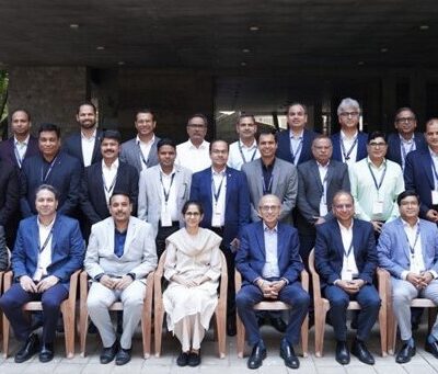
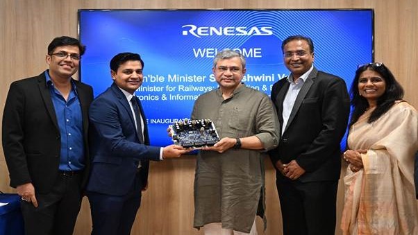
Bengaluru: In a landmark moment for India’s technology ambitions, Union Minister for Electronics and Information Technology, Railways, and Information and Broadcasting, Ashwini Vaishnaw, on Tuesday inaugurated India’s first 3-nanometer (nm) semiconductor chip design centres in Noida and Bengaluru.
These state-of-the-art facilities by Renesas Electronics India Private Limited mark a giant leap in the country’s semiconductor design capabilities, placing India on a par with the world’s most advanced chip innovators.
“Designing at 3nm is truly next-generation. We’ve done 7nm and 5nm earlier, but this marks a new frontier,” the Minister declared, underscoring the strategic importance of this milestone.
“With this, India signals to the world that it is no longer just participating in the semiconductor space — it is shaping its future,” he added.
The Noida facility, in particular, stands out as a flagship centre in Uttar Pradesh’s growing tech ecosystem. Together with the Bengaluru centre, these design hubs are expected to power innovations that will fuel next-generation computing, AI, telecommunications, automotive, and medical technologies.
A holistic semiconductor strategy
Vaishnaw outlined India’s comprehensive semiconductor roadmap that spans the entire value chain — design, fabrication, ATMP (Assembly, Testing, Marking, and Packaging), as well as the upstream ecosystem including equipment, specialty gases, and chemicals.
Citing India’s growing stature at global platforms such as the World Economic Forum at Davos, he noted increasing investor confidence with major players like Applied Materials and Lam Research already committing to India’s vision.
“The inauguration of this major semiconductor design centre is not just a milestone for Renesas or for Uttar Pradesh; it’s a key step toward creating a pan-India semiconductor ecosystem that taps into the deep talent pool across our engineering institutions,” said Vaishnaw.
Talent development at the core
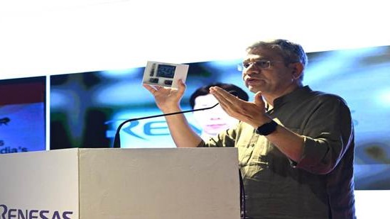
In a major announcement aimed at strengthening India’s future talent base, the Minister launched a new semiconductor learning kit tailored for engineering students. This hands-on hardware toolkit complements the advanced Electronic Design Automation (EDA) software tools already distributed to over 270 academic institutions under the India Semiconductor Mission (ISM).
“This integration of software and hardware learning will create truly industry-ready engineers. We are not just building infrastructure — we’re investing in long-term talent,” Vaishnaw stated, and lauded the efforts of CDAC and the ISM team in driving forward this national mission efficiently.
Strategic backing and global vision
The Minister credited Prime Minister Narendra Modi for recognizing semiconductors as a strategic sector under the Aatmanirbhar Bharat vision.
“Within just three years, we’ve transformed from a nascent ecosystem to an emerging global hub. The momentum is building at the right time, as demand for chips across sectors — smartphones, laptops, automobiles, defence, and healthcare — is set to explode,” he added.
Renesas reaffirms commitment to India
Speaking at the event, Hidetoshi Shibata, CEO and Managing Director of Renesas Electronics, called India a “strategic cornerstone” for the company.
He emphasized Renesas’ intent to deepen its end-to-end capabilities in India —from architecture and design to testing and validation.
“We see India not just as a talent hub but as a full-spectrum innovation partner. Our collaboration with the Government of India, support for over 250 academic institutions, and active participation in initiatives like Chips to Startup (C2S) and the Design Linked Incentive (DLI) scheme show our long-term commitment,” Shibata said.
He highlighted that the convergence of India’s engineering talent and Indo-Japan strategic collaboration could help redefine the global semiconductor lifecycle.
With the launch of India’s first 3nm chip design centres, a new era of innovation, manufacturing resilience and talent empowerment begins —strengthening the country’s position as a global semiconductor powerhouse.